Advanced PCB and Package Substrate Solutions for AI, HPC, and Semiconductor Test.

 Company Profile
FICT USA, Inc. is a wholly owned subsidiary of FICT LIMITED, a high-end PCB and substrate manufacturer.
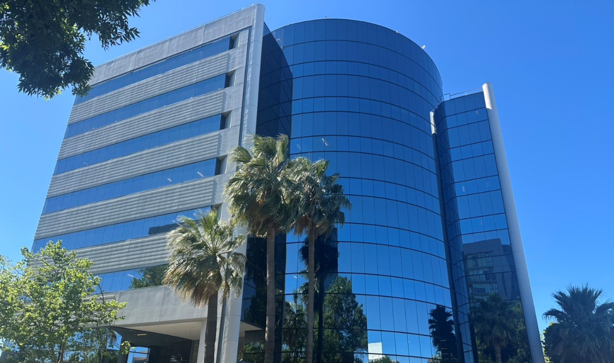
Based in San Jose, California, FICT USA is responsible for sales activities across North America and Europe and serves as a primary sales contact point for customers in liaison with FICT's engineering and manufacturing teams in Nagano, Japan.
|
Corporate Name |
FICT USA, Inc. |
|---|---|
| Location | 100 Century Center CT, Suite 302, San Jose, CA 95112, USA Tel. : 1-408-716-8972 MAP |
| Established | April 1st, 2026 |
| Business | Sales |

 Why FICT
FICT combines advanced interconnect technologies, proven manufacturing expertise, and application-focused support for customers developing high-performance and high-reliability systems.
 Advanced Interconnect Technologies
Powering the leap to 224 Gbps and beyond, FICT's proprietary interconnect platforms--F ALCS, G ALCS, and ALCS BBC--break through the limits of conventional PCBs. Engineered for next-generation AI and HPC, they redefine signal integrity, density, and scalable layer architectures for today's and tomorrow's designs. LINK
 Driven by Leading-Edge Requirements
FICT's long-standing relationships with industry leaders provide early visibility into emerging requirements, helping align technology development with the needs of next-generation applications.
 Cross-Technology Innovation
With skilled engineers and a deep base of accumulated knowledge across multiple technologies, FICT can integrate ideas from different applications, develop solutions beyond conventional approaches, and provide customized products tailored to meet specific customer needs.
 Proven Engineering and Manufacturing Expertise
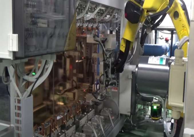
With over 60 years of PCB expertise, roots in Fujitsu's PCB division, and advanced High-mix, low volume manufacturing in Nagano, Japan, FICT combines technical depth with a strong culture of quality, precision, and continuous improvement.
 Applications We Support
FICT supports customers developing advanced systems for compute-intensive, high-performance, and precision-critical applications. Our solutions are designed to address demanding electrical, mechanical, and manufacturing requirements in next-generation architectures.
AI, HPC, and
Infrastructure
Systems
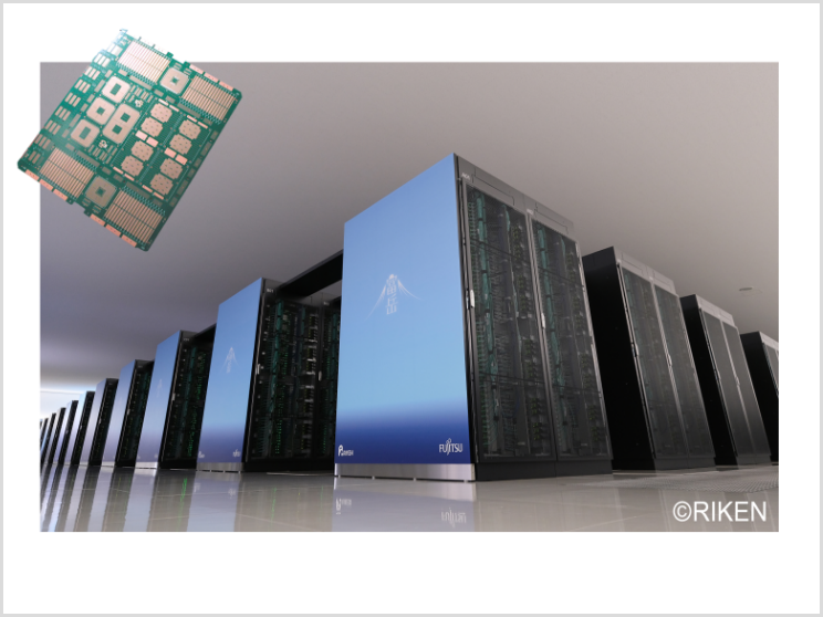
Advanced high-density and high-layer-count PCB solutions for AI, high-performance computing, high-end servers, and ICT infrastructure requiring high wiring capacity, signal integrity, low transmission loss, and long-term reliability.
- Key capabilities
-
- All-layer IVH structure
- HDI
- High wiring capacity
- Ultra-high-layer and high density designs
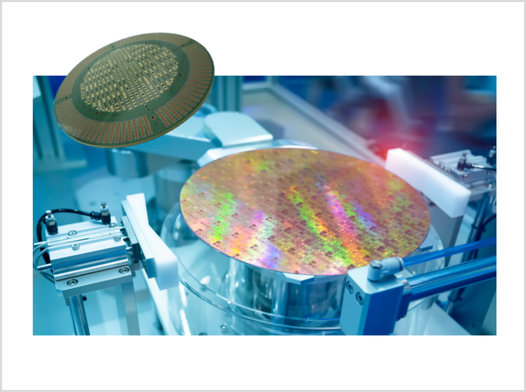
Advanced
Packaging

High-performance substrate solutions for servers, semiconductors, FPGAs, and advanced compute applications requiring high heat dissipation, high-current capability, high-speed signal transmission, and large-size package substrate support.
- Key capabilities
-
- High-mix, Low-volume production
- High heat dissipation
- High-current capability
Semiconductor
Test
Equipment
High-performance probe card PCB solutions for semiconductor test equipment requiring fine pitch, high pin count, high-speed testing performance, and reliable signal transmission in advanced test environments.
- Key capabilities
-
- Fine pitch
- High pin count
- High-speed testing
- Low-CTE materials
- MEMS-based solutions
 Advanced Interconnect Technologies
FICT's advanced interconnect technologies are designed to overcome conventional limitations in density, performance, and manufacturability for next-generation applications.
ALCS Series Technologies
All Layer Z-Connection Structure Technology
The ALCS series is FICT's proprietary technology platform for advanced interconnect structures. Developed to overcome the limitations of conventional PCB architectures, the ALCS series expands design flexibility, improves wiring density, and opens a path toward future multilayer and glass-based structures.
F-ALCS Technology
All Layer Z-Connection Structure Technology
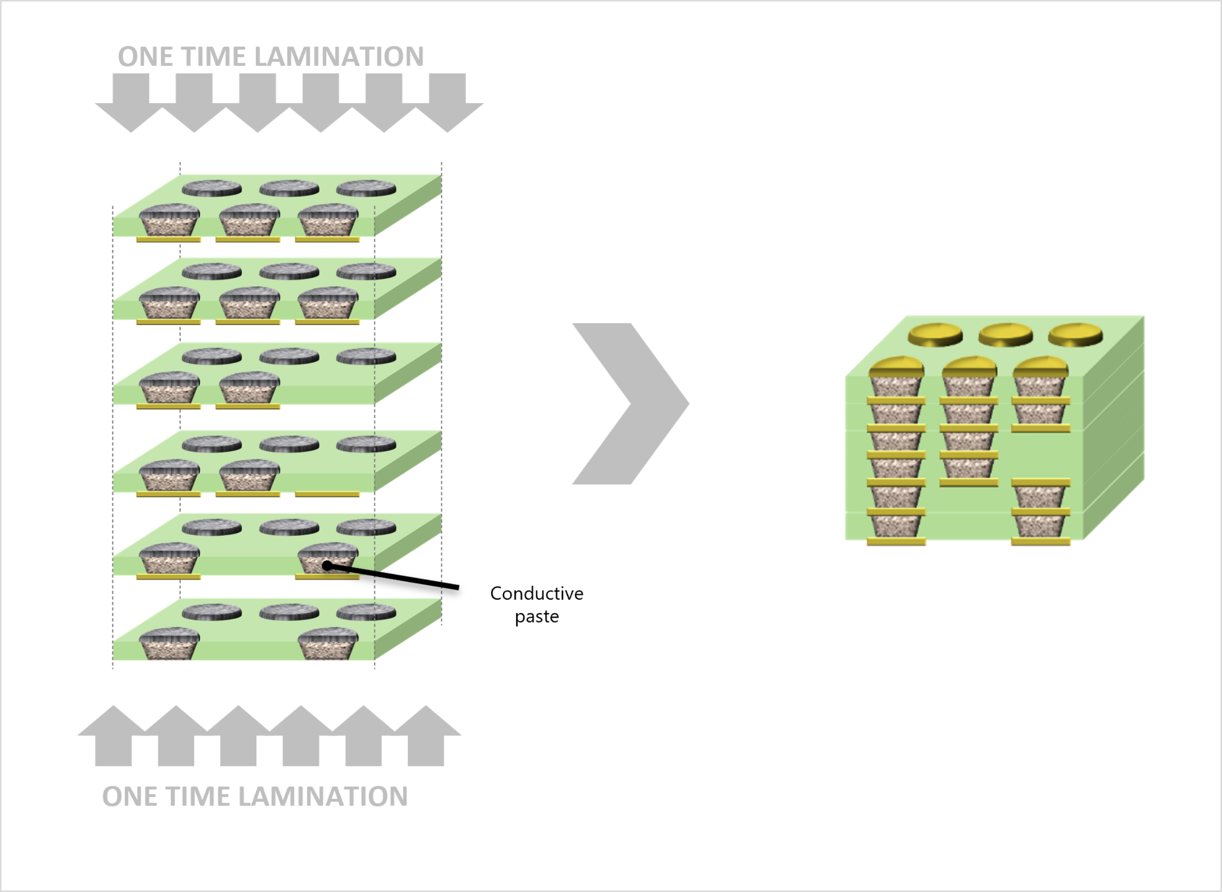
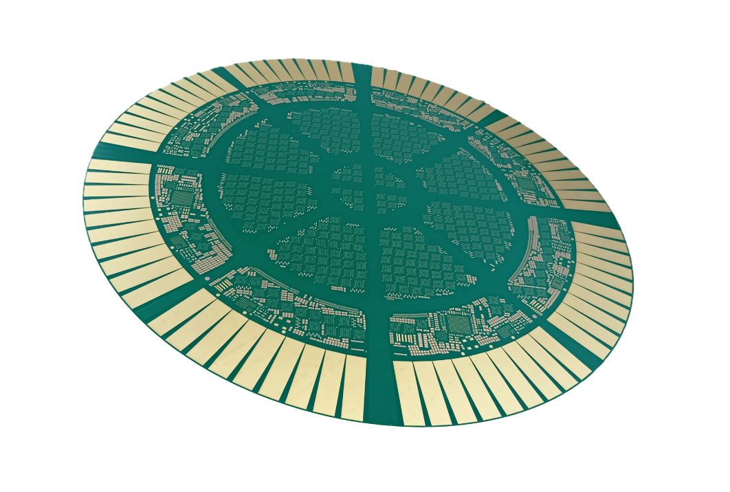
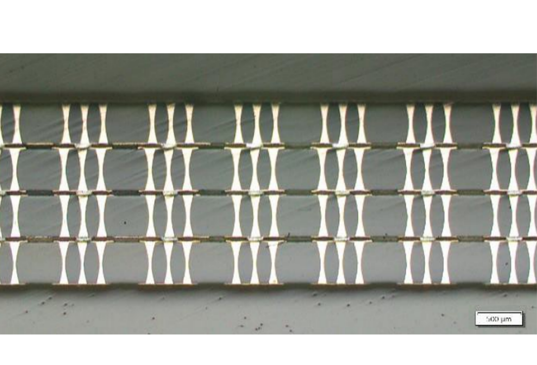
F-ALCS technology is a proprietary any-layer interconnect technology designed for high-density, high-speed PCB applications. F-ALCS enables all layers to be interconnected through a one-time lamination process, forming an Any-Layer IVH (Interstitial Via Hole) structure using a revolutionary conductive paste. This approach eliminates conventional stacking limitations and enhances design flexibility. Currently, the technology supports up to 72 layers in an any-layer IVH structure, achieving a total wiring capability equivalent to 140 layers. F-ALCS is well suited for demanding applications such as probe cards--including main boards and space transformers--as well as advanced high-multilayer PCB designs."
Sample
- All IVH with F-ALCS
Technology (64L) -
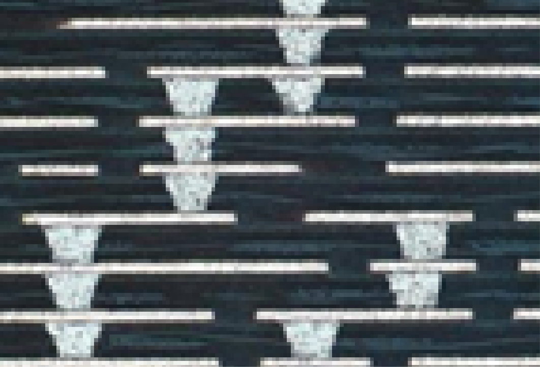
- Sample Picture
-
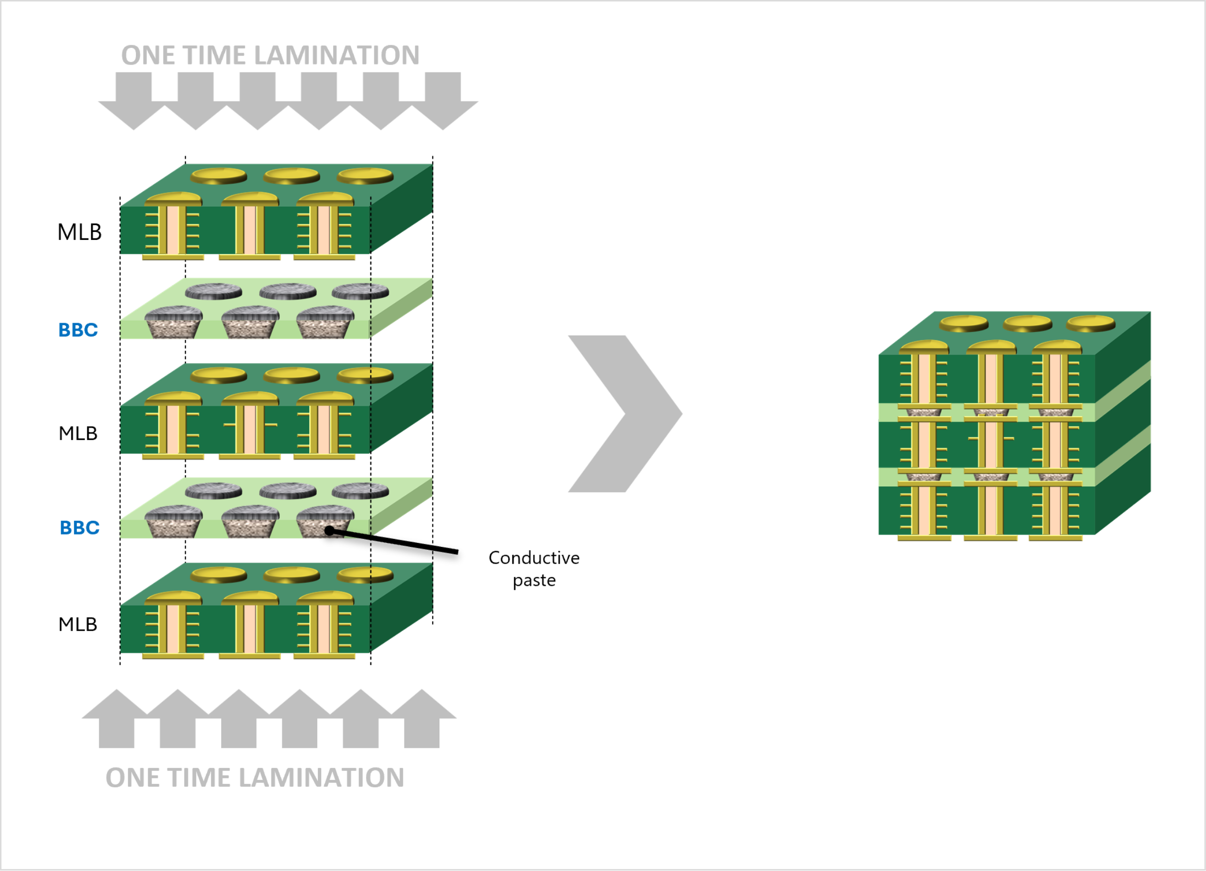
ALCS-BBC Technology
All Layer Z-Connection Structure Board to Board Connection Technology
As high-end DRAM testing continues to demand increasing layer counts, conventional PCB technologies face critical limitations due to aspect ratio constraints and material handling difficulties.
To address these challenges, FICT has developed ALCS-BBC technology. Unlike traditional methods, ALCS-BBC directly connects Boards together. This innovative structure makes it possible to achieve extremely high aspect ratio connections--such as AR66--and enables ultra-thick, high-layer-count designs, including structures with up to 160 layers and 10 mm thickness, surpassing the boundaries of conventional multilayer PCB technologies.
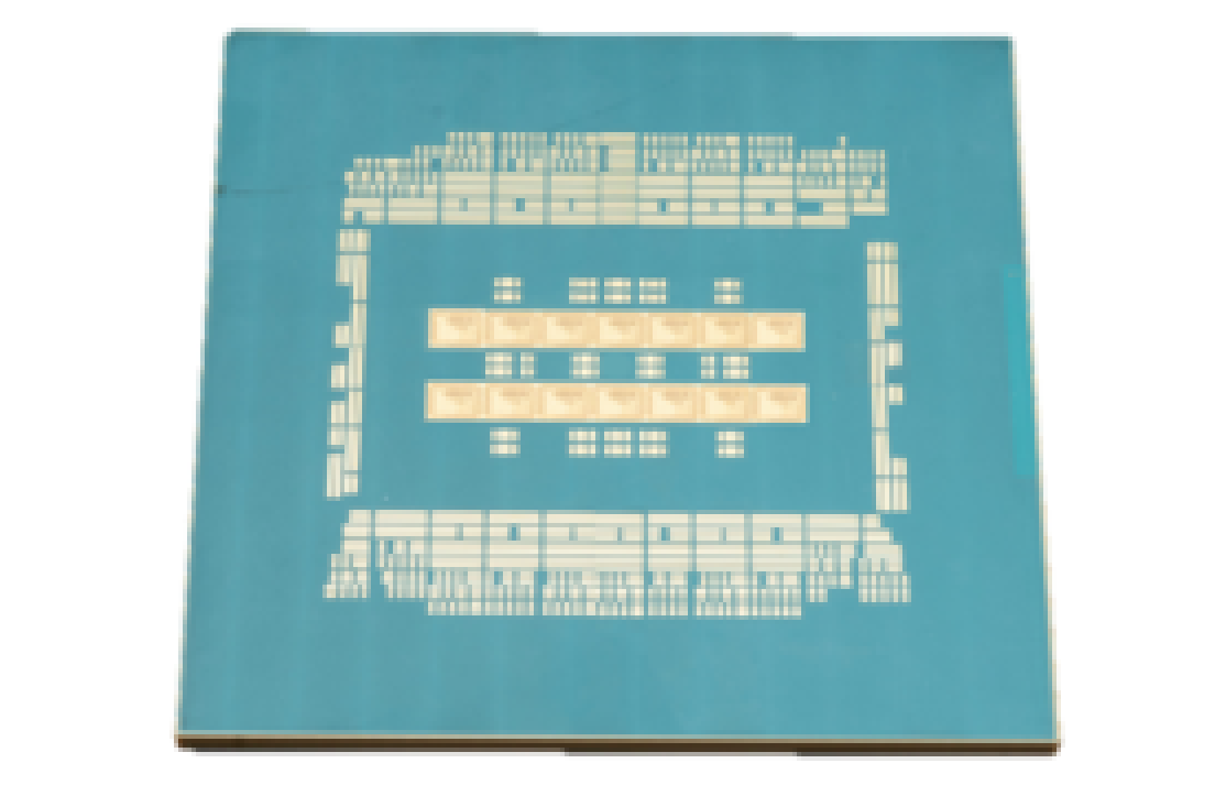
Sample
- Cross Section of 10mmt, 160
Layers ALCS-BBC PCB -
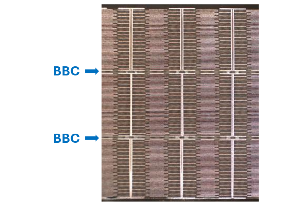
- Sample Picture
-
G-ALCS Technology
Glass All-Layer Z-Connection Structure Technology
As device demands shift toward high-precision optical integration and fine-pitch interconnects, conventional organic substrates fall short due to thermal expansion and warpage, driving to dimensionally stable glass-based solutions. While glass offers superior material properties, single-glass structures face challenges such as easy cracking and TGV reliability issues. To overcome this, FICT adopts a multilayer approach, combining glass with resin layers that absorb and disperse stress, significantly improving mechanical robustness and crack resistance. Building on this concept, G-ALCS introduces a low aspect ratio TGV stacked architecture that reduces stress between glass and copper plating, minimizes copper volume, and enhances reliability under thermal cycling. G-ALCS represents a promising technology currently being advanced through research and development at FICT's R&D centers.
Status: Under Development
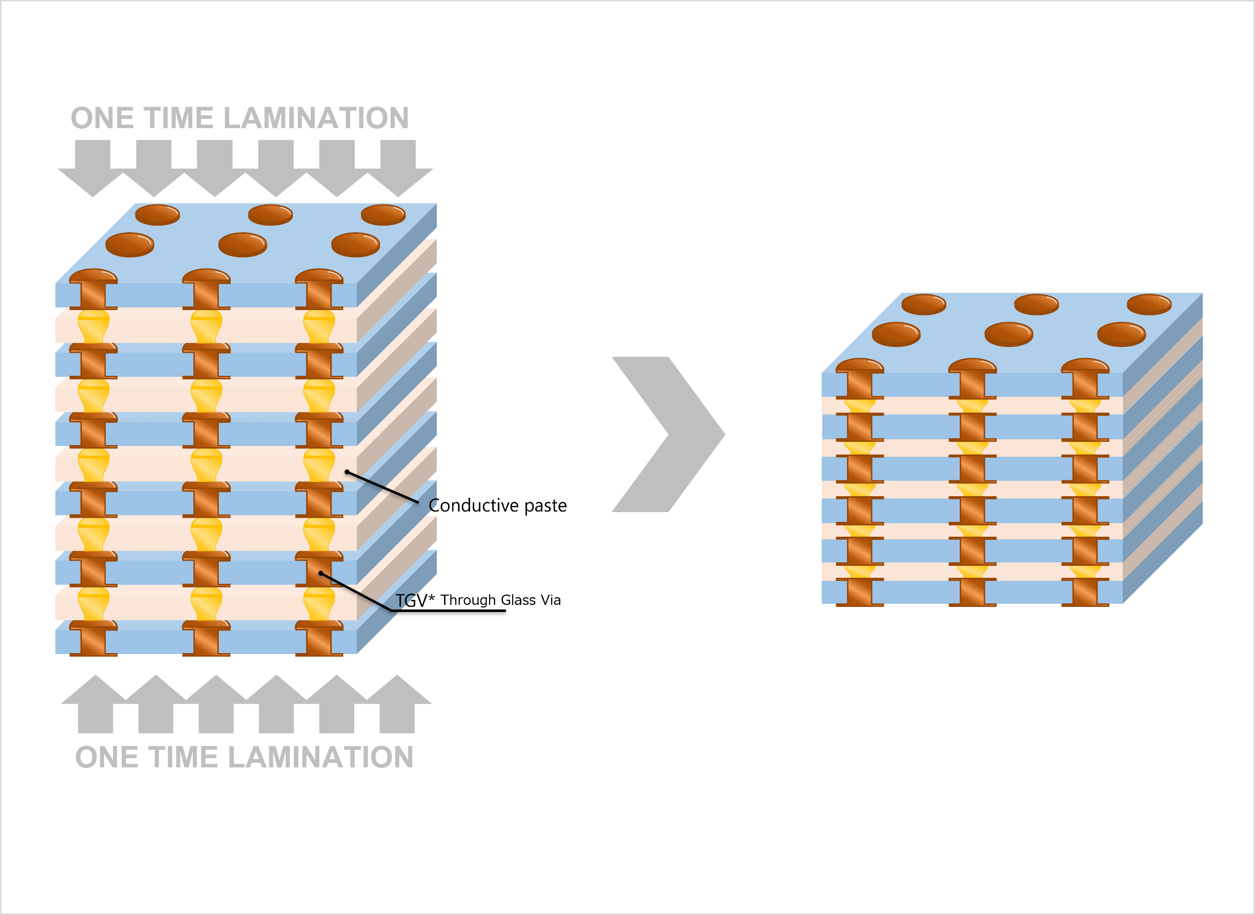
Sample
- 8L G-ALCS Cross Section
-
- Sample Picture
-
Space Transformer Organic Technology
FICT's Space Transformer Organic (STO) technology is designed to meet the increasing demands of advanced semiconductor testing. As devices become more complex, requirements such as finer pitch, higher pin counts, multi-DUT testing, and high-speed, high-power performance continue to grow.
To address these challenges, FICT develops high-density, highly reliable STO solutions featuring advanced build-up structures, precise C4 pad control, and low-CTE materials for improved stability.
With capabilities down to 20 µm DUT pin pitch and support for ultra-fine C4 pitch and multi-layer structures, FICT enables flexible, high-performance designs tailored to next-generation test requirements.
Our proprietary F-ALCS core technology further enhances design freedom and interconnection capability, supporting optimized solutions from development to mass production.
Sample
- Build-up 20 layers cross section
-
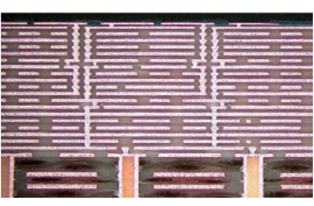
- Sample Picture
-
Contact Us