Solution Services
Board Design
 Board design
We provide turnkey PCB solutions from circuit design to PCB manufacturing.
And PCB design optimization for high-speed transmission with SI/PI board simulation. Cooling solutions for
product miniaturization with thermal, fluid and stress-strain analysis.
 Best Solutions for
Customer Problems
We provide concurrent PCB design solution that integrate electrical and thermal fluid/stress simulations for customer's product developments.
01
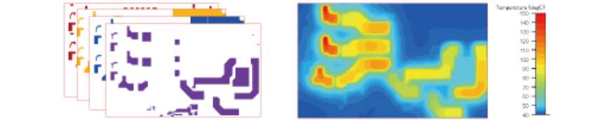
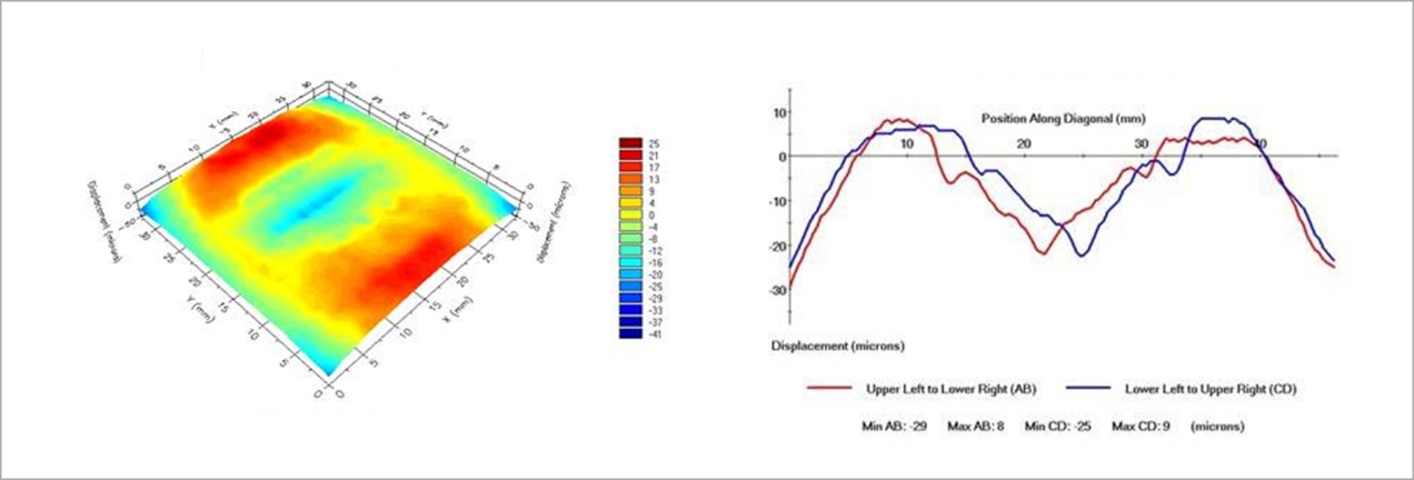
Design PCBs with low warpages
We perform warpage analysis, using Cu ratio model based on the real PCB designs. We propose optimized PCB designs low warpages whether BGAs are used.
Examples of PCB stress-strain analysis


02
Design PCBs with joule heat analysis for high current applications
We propose optimal PCB designs with thermal analysis that integrate joule heat and device operating heat analysis.
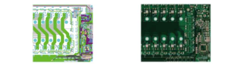
【1】Perform joule heat analysis with
precise trace pattern modeling
based on
the
real designs.
【2】 Improve trace flexibility with Embedded Bus Bar.
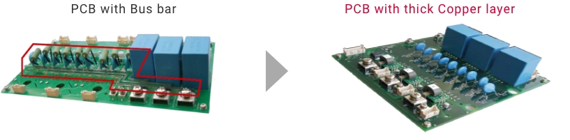
【3】Place control logic and power devices on the same surface layer.
03
Realize stable operation for high performance PCBs
Our optimized PCB design solutions for high performance applications reduce prototype cycles, lead-time, and cost.
【1】Suitable PCB specifications
Optimum materials, Layer structure and design rules
【2】Signal Integrity(SI)Analysis
Waveform quality and timing of high-speed DDRx interface.
【3】 Power Integrity(PI)Analysis
Check DC Drop and Input Impedance of Power Line for Digital Board.
【4】VG plane resonance analysis
Check VG plane resonance for Digital Board.

 Application Fields
We provide comprehensive design solutions for performance, miniaturization, and cooling in a
wide range of products, devices and modules.
With our extensive experiences in a wide variety of areas, we offer value-added design solutions for our
customers.
01
High performance PCBs for Super Computers, ICT Infrastructure and Medical
systems
| Board Size | 440 x 350mm |
|---|---|
| Structure | 24 Layers |
| Device counts | 8,400 |
| Device Pin counts | 39,000 pin |
| Wire counts | 30,000 wires |
More details for "High Density Interconnect PCBs"
Read More
02
High density PCBs for Automotive, mobile and IoT
| Board Size | 70 x 550mm |
|---|---|
| Structure | 12 Layers (5-2-5) |
| Device counts | 13,000 |
| Device Pin counts | 6,200 pin |
| Wire counts | 1,500 wires |
More details for
"HDI (Buildup) PCBs"
03
Thick Cu PCBs for Industrial and Power electronics
(Thick Cu for high current use)
| Board Size | 180 x 110mm |
|---|---|
| Structure | 4 Layers |
| Device counts | 60 |
| Device Pin counts | 250 pin |
| Wire counts | 160 wires |
More details for
"Thick Copper PCBs"
04
Semiconductor packaging substrates
| Board Size | 72 x 65mm |
|---|---|
| Structure | 20 Layer(6-8-6) |
| IO counts of DIE | 3,500 pin |
| BGA Pin counts | 30,000 pin |
More details for
"Package Substrate"
05
High layer count PCBs for Semiconductor tests
| Board Size | 100 x 100mm |
|---|---|
| Structure | 51 Layers(14-23-14) |
| Device counts | 6 DUT |
| Device Pin counts | 55,800 pin |
| Wire counts | 3,500 wires |
| Board Size | φ520mm |
|---|---|
| Structure | 76 Layers |
| Device counts | 28,700 |
| Device Pin counts | 107,500 pin |
| Wire counts | 35,600 wires |
More details for
"Probe Cards"
 Design Tools and Environment
We provide total PCB design solutions that include a wide range of simulations. We interface design data to a large variety of tools for electrical, thermal, and stress-strain simulations to add values to our customer's products.
CAE tools (CAD/CAE)

Simulation Tools

PCB Design Center
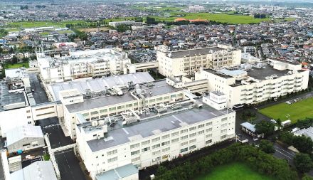
Nagano headquarters

Kawasaki office

FICT VIETNAM COMPANY LIMITED
 Electrical Simulation
We design the high-speed digital board using electrical simulation to satisfy Signal and Power Integrity.
Signal Integrity
SI simulation by using 3D electromagnetic field simulator
We design high-speed digital board using electromagnetic field simulation.
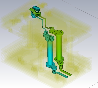
3D model of differential
signal for Module Board
Insertion loss "SDD21"
Return loss "SDD11"d
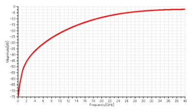
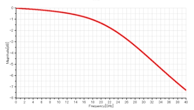
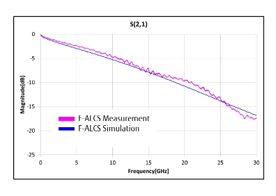
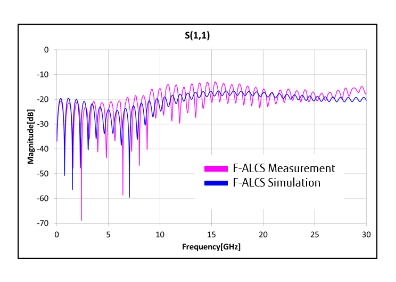
Example of transmission characteristics analysis of
F-ALCS structural substrate
The transmission characteristics analysis results and measurement results for the F-ALCS wiring structure are shown below.
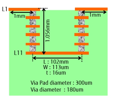
F-ALCS PCB Model
Insertion loss S21
Return Loss S11
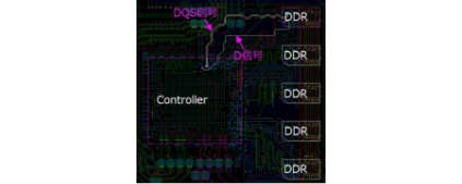
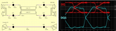
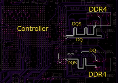
SI simulation for DDR SDRAM
We design board which satisfied Signal Integrity(SI) about DDR SDRAM Interface.
Simulator:COLMINA CAE Signal Integrity (FUJITSU)
DDR4 SDRAM Layout
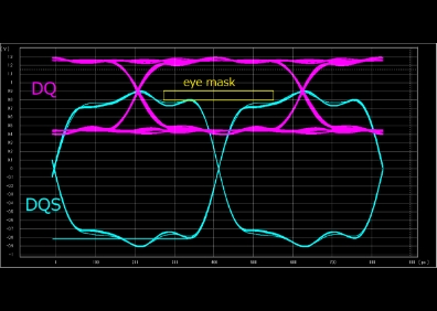
DQ and
DQS Signal's Topology
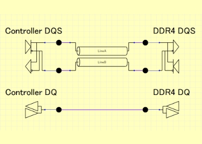
DQ and
DQS Signal's eye diagram
SI simulation for High speed digital channel
We design board which satisfied Signal Integrity(SI) about High speed digital channel.
Simulator:COLMINA CAE Signal Integrity (FUJITSU)
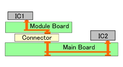
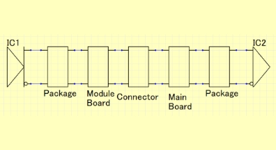
Interconnect between main
board andmodule boardt
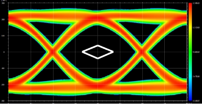
25Gbps signal's eye diagram
Channel Model
Power Integrity
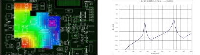
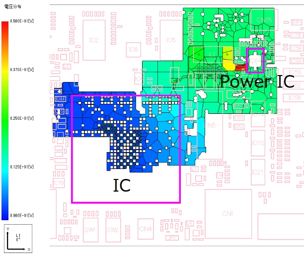
DC drop simulation
We propose optimized Power Distribution Network designs by electrically analyzing the VDD and GND net (PDN) from the power supply element (VRM) to the IC Devices.
Simulator:COLMINA CAE Power Integrity(FUJITSU)
DC drop simulation model
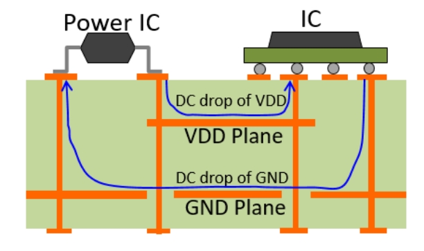
DC drop simulation result Voltage drop from Power IC to IC
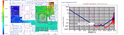
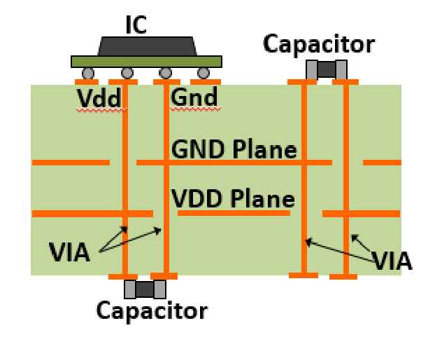
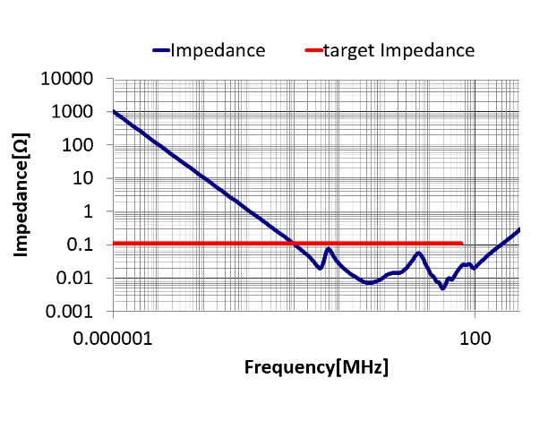
Impedance simulation
For a low power impedance, we propose the design of the power distribution network (PDN) including the VDD/GND plane, vias, and capacitor.
Simulator:COLMINA CAE Power Integrity(FUJITSU)
Impedance simulation model
Impedance simulation result
Impedance of PDN observed from IC
Physical Simulation
We support the optimization packaging design for the customer by our Thermal Management Analysis and Packaging Stress Analysis.。
Thermal Management Analysis
We perform verification and evaluation for thermal structure, responding to each customer's
thermal problems for electronic devices.
By performing our thermal management analysis in the early stages of the development phase, we help our
customers in reducing cost and time during the development process.
- Highly precise modeling
- Optimization of radiating fin shape
- Optimization of flow path structure and/or inlet/outlet port
- Numerical evaluation for unmeasurable fine structure
- Smooth modeling in collaboration with a variety of 3D tools(STEP, SAT, STL, iges, Pro/E etc.)
- Calculation of junction temperature by estimating temperature rise of electronic device
- Evaluation of cooling structure inside casing of electronic device
- Verifications of results represented by arbitrary cross-section distribution map and/or vector is available by visualizing flows for temperature/speed/fluid
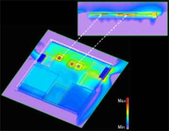
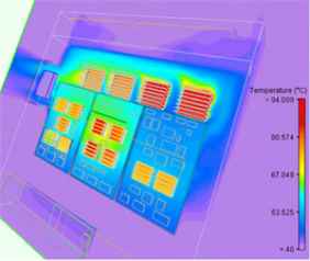
Temperature distribution of laptop PC
Analysis Tool:FLOTHERM
Temperature distribution representation
Air speed distribution representation
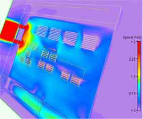
Flow representation
Flow representation (Enlarged view)
Packaging Stress Analysis
The heat generated at the time of component packaging causes substrate warpage and gives
stress on the component joints, decreasing packaging yield and product reliability. Analyzing such
problems in packaging in a way consistent with customer's point of view, we propose optimal packaging
design by suggesting packaging location and stress improvement countermeasure best suited to each
customer.
Performing simulations in the early stages of the development phase will greatly reduce the number of
verifications for prototypes, resulting in the reduction of cost and time during the development process.
- Fully utilize the extensive experience and performance of our company and Fujitsu Group combine
- Provide non-linear analysis and coupled analysis that take into account the temperature dependency of various material physical property value
- Accommodate highly precise analysis, providing large-scale analysis by mesh refinement
- Perform qualitative and quantitative verifications based on visualization and quantification of stress/strain distributions
- Perform highly precise life prediction by matching simulation and actual devices
- Perform modeling in collaboration with a variety of 3D tools(Pro/E, VPS, step, iges, inp, etc.)
Type of Analysis
- Stress and thermal stress analysis
- Warpage behavior simulation
- SMT board level reliability analysis
- Dynamic shock analysis
- Structural strength analysis
- Vibration analysis
- Modeling service for simulation
Analysis Tool:・ABAQUS(/Standard,/Explicit)
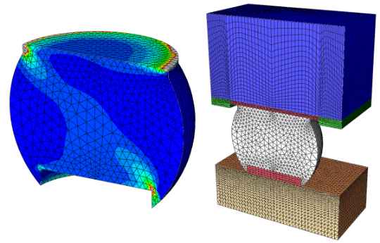
【1】Case Example : Stress Analysis by Heat/Structure Interaction
Evaluate lifetime by calculating lifetime test acceleration factor based on plastic strain analysis of solder bump.
note) ABAQUS : registered trademark of Dassault Systèmes.
Temperature distribution analysis
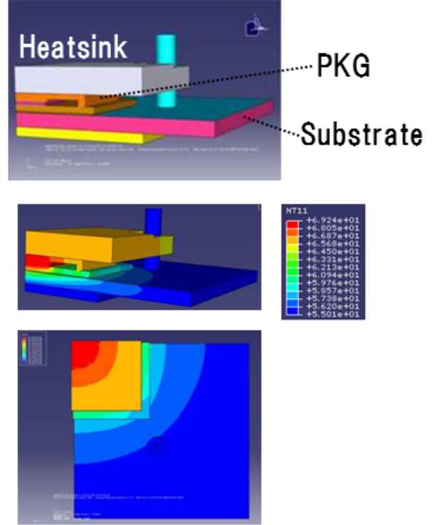
Thermal cycle test
Power cycle (Actual Performance)
Zooming analysis
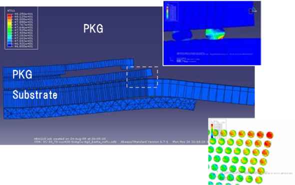
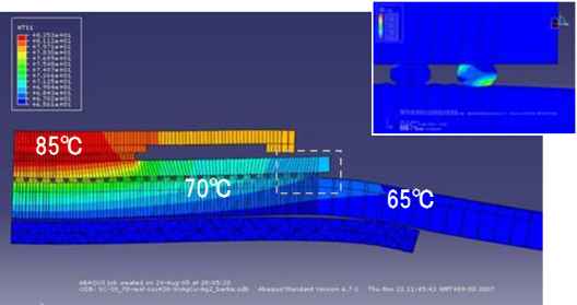
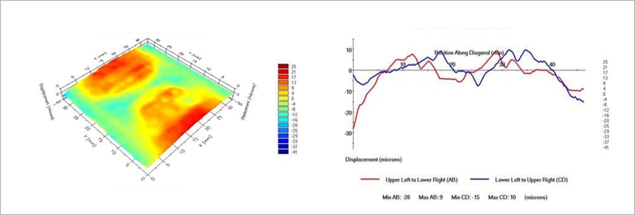
【2】Case Example: Warpage Behavior Analysis of PWBs
Propose optimal pattern design to reduce connection failure resulting from warpage by analyzing substrate warpage behavior caused by the heat at the time of component mounting.
Warpage behavior analysis
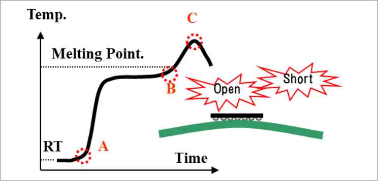
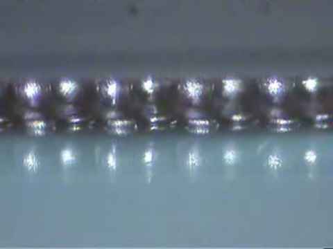
Example of BGA disconnection
At room temperature (A)
At reflow temperature (B-C)
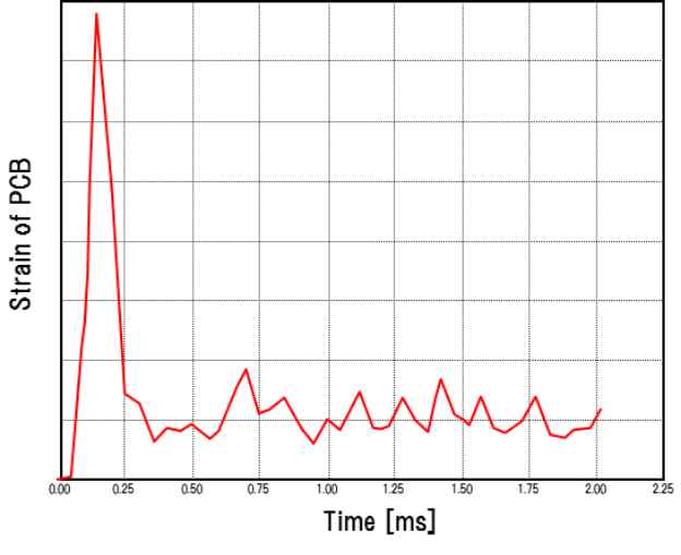
【3】Case Example: Dropping Impact Analysis
Distortion distribution of assembled printed circuit board under dropping impact
will be analyzed.
Proof stress through dropping impact will be evaluated from these impact strain
simulation.
Distortion distribution of assembled printed circuit board, especially, precise analysis of neighborhood of IC package
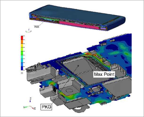
Strain behavior of dropping impact with millisecond time at neighborhood of IC package
Advanced Technologies
Back to top
Product
Back to top
Solution Services
Back to top
Technical Services
Back to top