Product
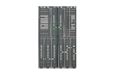
HDI PCBs
 Product
We provide total solutions from design and mounting simulation to substrate manufacturing for high-performance and high-speed transmission equipment such as the latest communication equipment.
 Best Solutions for
Customer Problems
In order to meet the demands for higher performance of the latest information communication equipment and modules, we solve customer problems not only with printed circuit boards but also with solutions for the entire equipment.
01
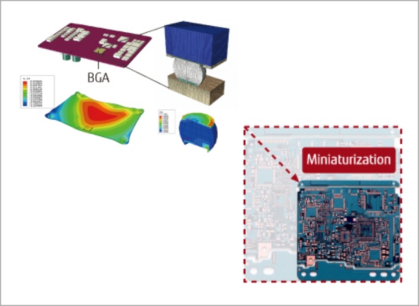
How to reduce product size to 50%
We offer optimal PCB solutions with rigid, thin and lightweight materials to realize the miniaturization of the product. We propose stress-strain analysis to solve warpage problems that associated with the product miniaturization and also the junction reliability problems for device mounting.
More details for "Stress Analysis"
Read More
02
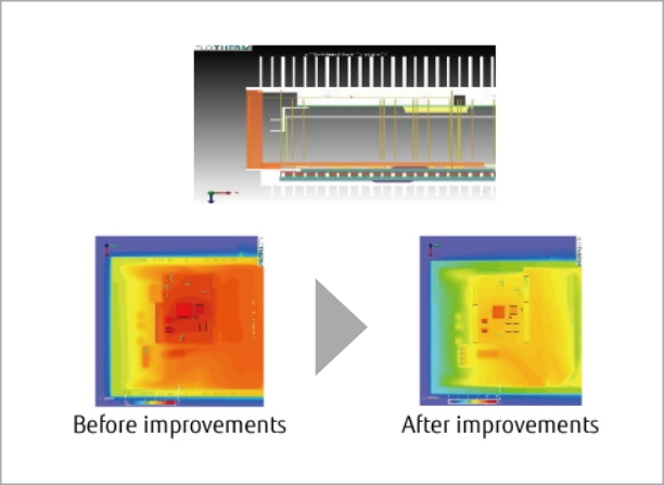
Thermal problems associated with the miniaturization
We provide total solutions with our thermal and fluid analysis for the cooling problems of heat spot occurred by the miniaturization.
More details for "Thermal Management Analysis"
Read More
 Application Fields
01
Buildup PCB for Communication Infrastructure
| Layer Construction | 3-6-3 |
|---|---|
| Via diameter | Φ0.10mm |
| Line/Space | 100µm/100µm (inner layers 80µm/100µm) |

02
Buildup for Handy Terminal
| Layer Construction | 1-8-1 |
|---|---|
| Via diameter | Φ0.08mm |
| Line/Space | 75µm/100µm (inner layers 75µm/75µm) |

03
Buildup for Semiconductor Related Equipment
| Layer Construction | 1-28+28-1 |
|---|---|
| Via diameter | Φ0.10mm |
| Line/Space | 100µm/150µm (inner layers 76µm/150µm) |
 Outline of PCB Specifications
- Buildup up to 3-n-3
- Via menu Filled Via, Stacked Via, etc.
- Structure 4 to 28layers+ 4 to 28layers
Buildup PCB(3-n-3)
Buildup and Lamination (1-n+n-1)
Advanced Technologies
Back to top
Product
Back to top
Solution Services
Back to top
Technical Services
Back to top