F-ALCS technology, which uses no plating process for vias forming, maximizes wiring capacity with its any layer IVH structure. This technology also enables to shorten fabrication lead-time with its one-time lamination process.
Product
Multilayer PCBs
We provide multilayer PCBs for
high performance products
such as ICT infrastructure
equipments which require
reliability
for long periods of time.
 High Density
 Interconnect PCBs
 High Density Interconnect PCBs
We provide total PCB solutions tailored to our customers needs and requirements for High-end Servers, Network systems and Infrastructure systems.
 Best Solutions for Customer Problems(High Density Interconnect
PCBs)
Best Solutions for Customer Problems(High Density Interconnect
PCBs)
01
Placing different high pin-count BGAs, on both side of the PCB
We propose high-density and high-reliability multilayer PCBs for large pin-count BGA, placement on both sides of PCBs, applying technologies of conventional and sequential lamination. Our extended IVH technology enables to apply sequential lamination technology even for large PCBs over 500mm size.
MV-3* structure
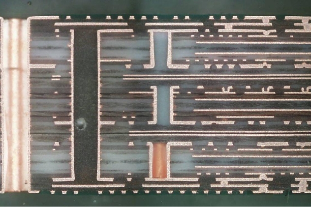
28 layers(14+14)
Note: *1) High density PCB fabrication technology for hybrid layer structure composed of HDI technology and sequential lamination process.
03
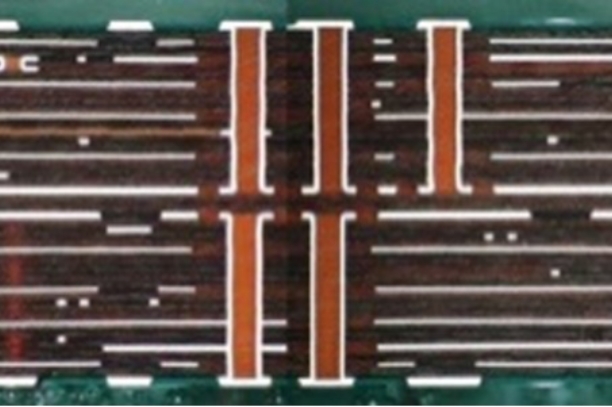
Fine Pitch through-hole-type multilayer PCBs
Narrow pitch PTH VIAs are available for high-density LSI testing boards and 0.4mm / 0.5mm pitch BGA burn-in boards. Moreover, high density PTH placements are available with our high-aspect PTH plating technology. General specifications about PCB thickness and their related PTH Via diameter are listed as below. We propose for customer needs beyond general specifications. Please contact our sales for further requirements.
Design Rule


For through-hole
mount device
8 layers(PTH φ0.15mm)
Thickness 1.6mm
For surface mount
device ※1
8 layers(PTH φ0.15mm)
Thickness 1.6mm Note:※1)PTH via in PAD structure
Ultra-high
layer-count PCB
50 layers (with 2 layers IVH)
Thickness 7.2mm
 PCB Application Fields &
Specification Outline
01
IVH PCBs for High performance Servers
| Layer Construction | 50 Layers (2 L with IVH) |
|---|---|
| PCB Size,Thickness | 568mm×470mm, 7.3mm |
| L/S, Via diameter | 90µm/110µm, φ350µm |
02
PCBs for 0.4mm pitch CSP burn-In tests
| Layer Construction | 8 Layers (for DIP type sockets) |
|---|---|
| PCB Size,Thickness | 480mm×580mm, 1.6mm |
| Via diameter | φ150µm |
 High Speed
 Transmission PCBs
High Speed Transmission PCBs
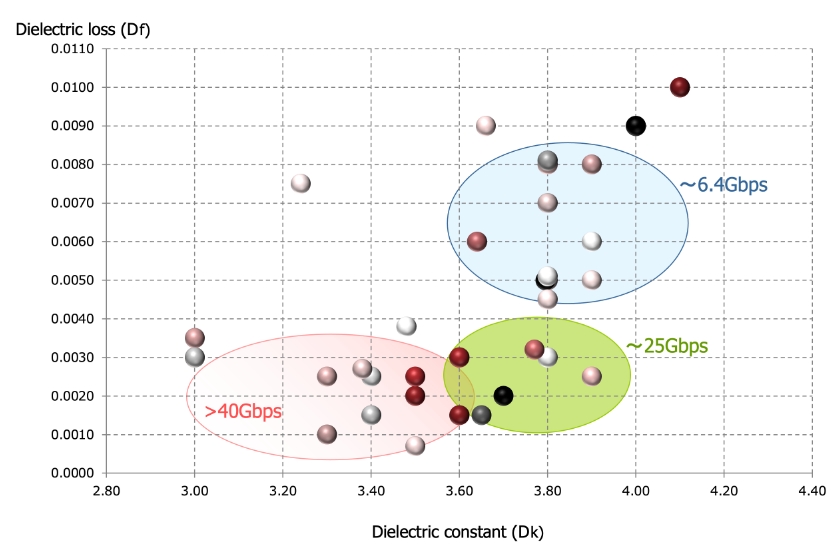
We provide high-performance multilayer PCBs, enabling ultra-high-speed transmission, with the latest technology to minimize transmission loss at high frequency by the PCB structure, decreasing open Via-stub. The high-speed transmission over 40Gbps is achieved by overall technology of the pattern surface smoothing, the back-drilling fabrication and the low loss dielectric material optimization.
Best Solutions for Customer Problems
01
PCB structure for high speed transmission
Material and structural optimization with accurate alignment technology for sequential lamination PCB enables high-speed transmission PCBs, tailored to customer needs and expectations.
- Supporting product development from the early stage of the design according to the electrical simulation and the real measurement data of transmission.
- Enabling low cost design with conventional and sequential lamination structure by different dielectric materials.
- Tight impedance control for the critical signal patterns enables high speed transmission, aiming for up to 50Gbps transmission.
Application of various low
loss materials
02
Transmission-loss improvements without changing materials
Smoothing the surface of the signal pattern with our technology enables significant improvement on transmission loss without changing dielectric materials to high specification.
Significant improvement on
transmission loss with chemical
bonding
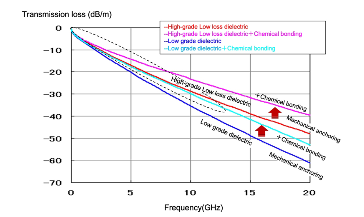
Smooth Pattern Technology (Comparison between mechanical anchoring and chemical bonding)

03
Stub-less VIA structures, minimizing reflection losses
Our back drilling technology, decreasing open-stub length, reduces the transmission loss by reflection noise at high frequency operation. And stable high-speed transmission can be achieved.
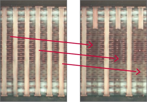
PCB cross section, applying back drilling technology
Double sided press-fit connector for high-speed transmission can be applied with comprehensive technology by back drilling and sequential lamination technology. Press-fit connectors, mounted from both sides, shorten wiring length and increase wiring density.
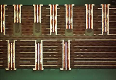
Backplane for double sided press-fit connector mounting
Sequential lamination PCBs with hybrid dielectric materials enables low loss dielectric material layer, applied only to necessary surface layers for the high-speed signal transmission. And its combination with the back drilling technology reduces transmission loss by reflection noises at high-speed transmission.
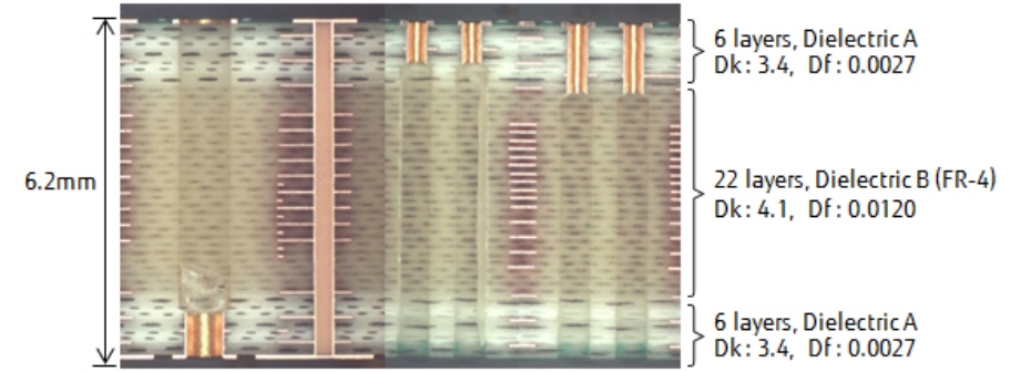
Sequential lamination structure with different 2-types of materials

PCB Application Fields &
Specification Outline
01
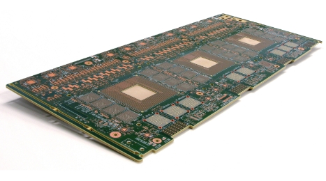
CPU Memory Board for Supercomputers
| Layer Construction | 22 layers |
|---|---|
| PCB Size, Thickness | 452mm×192mm, 3.068mm |
02
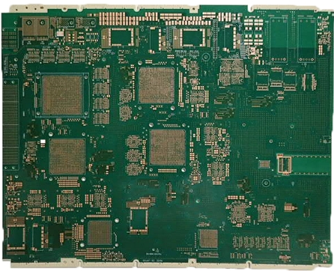
Sequential lamination PCBs for Network Infrastructure Systems
| Layer Construction | 28 layers (14 + 14) Sequential lamination |
|---|---|
| PCB Size, Thickness | 480mm×420mm, 3.6mm |
| Line / Space | 100µm/150µm |
| Via diameter (PTH, IVH) | φ350µm, φ120µm |
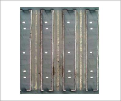
 Thick Copper PCBs
Thick Copper PCBs
We provide thick copper and good thermal conductive PCBs for large electric current applications of industrial systems, automotive and power electronics products. We propose best PCB solutions, applying copper coin technology and good thermal conductive materials for cooling high power devices.
Best Solutions for Customer Problems (Thick Copper PCBs)
01
PCBs for Large-Current Applications
We provide thick copper PCBs with maximum 500μm for large-current applications.
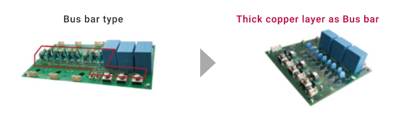
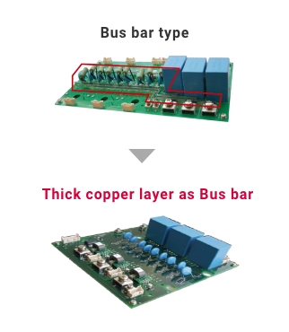
Using Thick Copper PCBs instead of Bus bar enables flexible wiring and better electrical insulation for large current traces.
Products miniaturization is achieved by the joule heat analysis of large-current patterns and the optimization of PCB design.
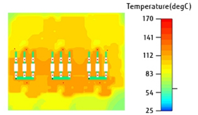
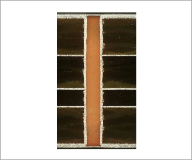
PCB temperature distribution analysis
<using 500μm Cu thickness>
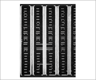
Optimized combination of inner copper thickness is enabled.
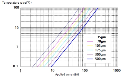
Thermal simulation of thick Cu pattern
Thick copper PCB(500µm max) for high current application
Thick copper PCB(1000µm max) for high current application (Under development)
02
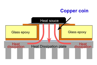
Cooling High Power Devices from backside of PCBs
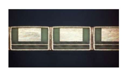
A highly effective heat conducting path is formed with the copper coin between PCB top and bottom, which enables to conduct the heat generated from the device efficiently to the opposite side of PCBs.
Embedded Copper coin product
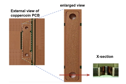
Image of device heat radiation,
using Copper coin
03
Spread heat spots onto PCBs
Applying high heat radiation material to PCBs enables significant improvements in conduction of heat to horizontal direction (x-y axis). As the electrically insulated high heat dissipation material is applied to PCBs, the high heat spots from power devices is distributed in the horizontal direction.
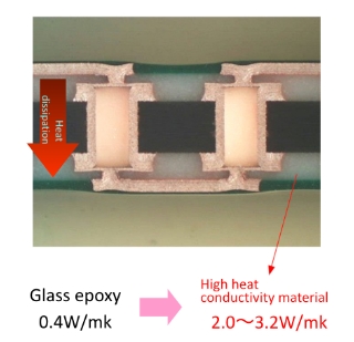
High heat dissipation PCB structure
04
Optimization of heat radiation on PCBs
We propose the best PCB technology solution for various demands for large current and high heat radiation. The feature of our PCB technology is shown as below.

PCB Application Fields &
Specification Outline
01
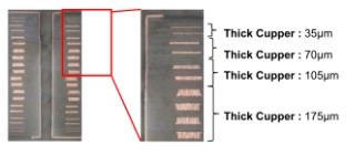
PCBs with 175µm thick Cu for LSI tester
| Layer Construction | 22 layers |
|---|---|
| PCB Size, Thickness | 599mm×694mm, 6.36mm |
| Copper Thickness (Inner layers) | 35µm, 70µm, 105µm, 175µm (4 types) |
02
High heat dissipation PCBs for Automotive
| Layer Construction | 8 layers(2-4-2) |
|---|---|
| PCB Size, Thickness | 320mm×192mm, 1.2mm |
| Line/Space | 100µm/100µm |
| Thermal conductivity | 1.5-2.5W /(m・K) |
03
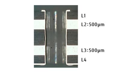
PCBs with 500µm thick Cu for large-current applications
| Layer Construction | 4 layers |
|---|---|
| PCB Size, Thickness | 147mm×145mm, 2.75mm |
| Line/Space | 200µm/150µm |
| Copper Thickness (Inner layers) | 500µm (L2, L3) |
Advanced Technologies
Back to top
Product
Back to top
Solution Services
Back to top
Technical Services
Back to top