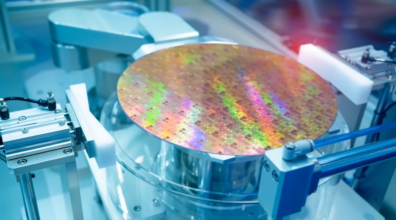
Advanced Technologies

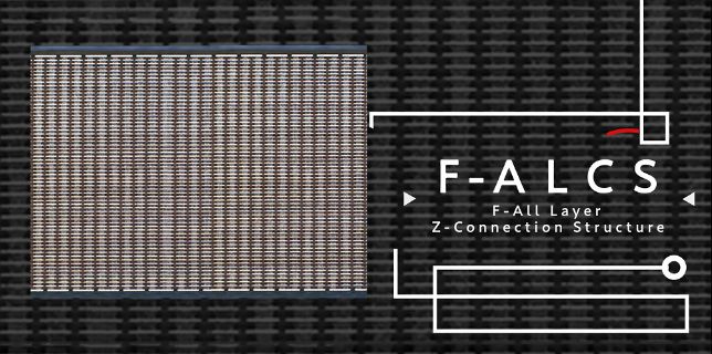
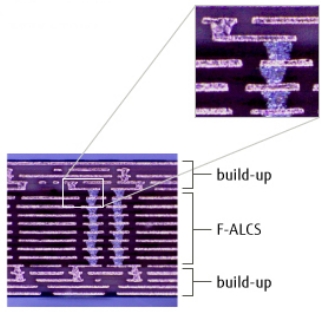
F-ALCS (All Layer (Z) Connection Structure) is our innovative plating copper less via formation PCB technology that enables high-speed signal transmission.
 F-ALCS
This technology has been gaining attention with its impressive capabilities in maximizing the PCB wiring capacity by enabling ultra-high multilayer and high-density wiring with its unique conductive paste.
This revolutionary conductive copper alloy makes it possible to connect all the layers together in a one time lamination to form an Any Layer IVH (Interstitial Via Hole) structure.
With the dramatic evolution of information technology such as cloud computing and AI, demand for data centers continues to grow at a rapid pace. 5G which supports high-speed and high-capacity data communications in the digital society and ICT supporting social infrastructures such as optical communications, are also flourishing rapidly.
These technological advancements have created an immense complexity in the manufacture of high multilayer, high density and low transmission loss PCBs for advanced data processing equipment.
The industry is adapting different approaches to overcome these challenges.
Our approach was to develop the F-ALCS technology to keep up with the need of the rapidly changing information society by providing a higher design freedom in alignment with the escalating environmental concerns of our times.
Product Introduction Video F-ALCS

 4 main Benefits of F-ALCS Technology
01
High degree of PCB Design freedom
The core advantage of F-ALCS technology lies in its design flexibility. Our F-ALCS enables the placement of vias (holes for electrical connection between layers) only on the required layer. The technology also allows the reduction of via in pads diameter which increases the possibilities for parts placement. By removing these two constraints, the available area for wiring can be greatly expanded.
Currently the technology enables up to 72 layers any layers IVH structure with the wiring level of 140 layers.
Surface Mounting area expansion
To create a transmission line in regular IVH PCBs, through holes need to be drilled from the top and bottom side of the PCB. This creates inevitable holes on the board surface which result in the reduction of available mounting surface.
By placing vias only on the needed layers to then laminate all the layers together in a one-time lamination with our conductive paste, F-ALCS lifts the mounting area design limitations encountered with the regular structure.


Wiring Capacity improvement
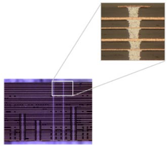
As shown in the comparison figure below, by pasting the layers together, F-ALCS enables the placement of as many vias a necessary in the desired part, avoiding the though hole that cause wiring restrictions (open stubs). This makes it possible to increase the wiring route and density by removing unnecessary vias in the internal structure of the PCB.


02
Transmission loss and reflection loss reduction for a High-speed signal transmission
As the realm of high-speed communication pushes the boundaries, signal transmissions now soar beyond 100 GHz. However, the conventional through-hole stub introduces a disruptive interference within this wavelength. In contrast, by using our conductive paste, our any-layer IVH (Interstitial Via Hole) technology approach stands as a stubless solution, facilitating uninterrupted high-speed transmission.
Our all-layer IVH technology prevents the generation of stubs at the via level that interfere with high-speed signal transmission. By reducing the return loss, transmission characteristics up to high frequencies can be obtained and faster signal transmission can be expected.
The figure below compares the transmission characteristics between F-ALCS and Conventional PCB structures.
By realizing an All layer IVH structure, our F-ALCS technology eliminates unnecessary via stubs. By reducing open stubs that reduces the transmission and reflection losses, this technology makes it possible to achieve an excellent transmission characteristic making it appealing for PCB for high-performance AI servers and 5G communications devices that require high-frequency capacity.
Transmission Characteristics Comparison between
F-ALCS and Conventional PCB structure

03
One-time lamination for a 50% process step reduction
Traditionally, we count 10 manufacturing process steps to manufacture regular IVH PCBs, from the formation of the wiring of the inner layer to the formation of the surface layers, including the plating process and sequential lamination. However, with F-ALCS the process consists in using the conductive paste to wire the inner layer in parallel after forming IVH by laser drilling. All via connections are then completed by performing a one-time lamination. This new manufacturing cuts out manufacturing steps to 5 steps, leading to a shorter delivery time.
Manufacturing process steps comparison
between Regular IVH PCB and F-ALCS PCB

04
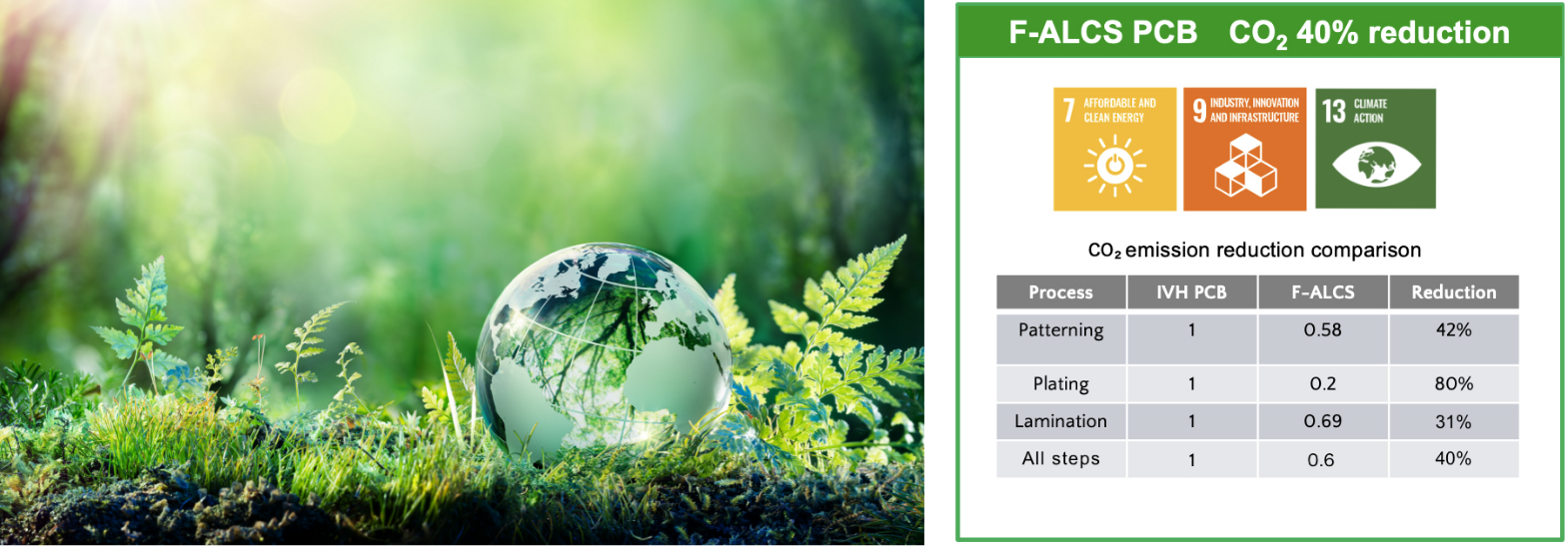
Environmentally friendly process without the Plating process; 40% CO₂ emission reduction!
The distinctiveness of this technology lies in its alignment with the escalating environmental concerns of our times. Given the contemporary emphasis on sustainability, we search for alternative process solutions to reduce wastewater treatment and electricity consumption as much as possible.
Our original technology ALCS is unique in terms of ecological friendliness since it doesn't require a plating stage. By opting for the conductive paste printing process for the via connection, waste liquid treatment such as plating solution is avoided.
Choosing this technology has proved the reduction of running costs (water, electricity, and processing time) and CO2 emissions during the manufacturing process by approximately 40%.
We are committed to providing environmentally friendly products through environmentally friendly F-ALCS manufacturing processes.
Customer feedback
Here are some testimonials from our customers who used the F-ALCS technology.
-
Managed one of the newest semiconductors with
high density wiringAs the integration of semiconductors increased, the amount of required wiring in a printed wiring board for wafer test has also increased. We were having trouble with the former printed wiring board design because the wiring density had reached its limit.


By using the F-ALCS, we were able to have higher wiring
density on the printed wiring board which made it possible
to have our semiconductor test done. -
Shortened delivery time by shortening development time
We often had to adjust our work schedule with our client due to the fact that we couldn't make the deadline they required, because we had to wait for the former high layered, high density printed wiring boards to be supplied.

Printed wiring boards with the F-ALCS technology has
made it possible for us to meet the deadline our client sets
because it doesn't require as much design and production
time as the former printed wiring boards. -
Enable high frequency transmission without open circuited stubs
The speed of signal transmissions on our printed wiring board needed to be increased because the speed of network systems has been accelerated. However, the solution to this issue was difficult to resolve because reducing the open circuited stubs in vias was quite challenging.

With the F-ALCS technology that adopts the all layer build
up structure, designing a printed wiring board has become
easier because we don't have to worry about creating open
circuited stubs.
Technology Application Case
01
High-density PCBs for ICT infrastructure (F-ALCS)
The size of PCBs for High-end servers, 5G infrastructure, and HPC is expanding, and consequently the need for high density wiring capacity increases. The core advantage of F-ALCS technology lies in the Any layer IVH process that dramatically improves the wiring capacity. In addition, because of the one-time lamination method, our technology will reduce the delivery time.

Specification
| PWB size | φ480mm |
|---|---|
| Construction | 76 layers |
| Pad pitch | 495µm |
| Pad diameter | φ300µm |
| Via diameter | φ180µm |
| Dielectric thickness | 100µm |
| Thickness | 7.4mmt |
Structure
<X-section>
02
Probe card for semiconductor test devices (F-ALCS+Buildup)
The increasing number of pins and progression to a finer pitch in probe card resulted in the demand for larger number of wires and more that 16-layer one sided buildup.
By adopting F-ALCS technology to structure the core part, we can dramatically improve the wiring capacity, and as a result, the number of build-up layers can be minimized to reduce the total number of layers.
Specification
| PWB size | □150mm |
|---|---|
| Construction | 28 layers |
| Pad pitch | 280µm |
| Pad diameter | φ170µm |
| Via diameter | φ110µm |
| Dielectric thickness | 60µm |
Structure
<X-section>
Product Application
Our F-ALCS technology can be applied to the Products below :
Related Technologies
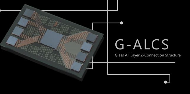
Through our F-ALCS technology initiative, we are working toward the integration of a glass substrate into the semiconductor packaging with our G-ALCS (Glass All Layer Z-Connection Structure) technology, opening new avenues for advancement.
To know more about our G-ALCS technology, download our catalog by submitting the catalog form below.
Product Introduction Video G-ALCS
Advanced Technologies
Back to top
Product
Back to top
Solution Services
Back to top
Technical Services
Back to top