Product
Probe Cards
 Probe Cards
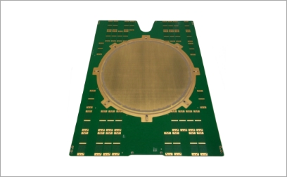
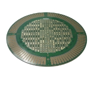
Our state-of-the-art technology provides innovative organic PCBs, best suited for probe cad applications with huge wiring capacity over 10000 nets, achieving high-quality signal integrity.
 Best Solutions for
Customer Problems
We propose the best solutions for the most advanced semiconductor device testing, based on our know-how and technologies accumulated over half a century.
01
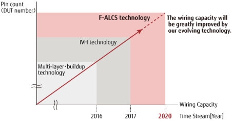
Maximization of wiring capacity
Any layer IVH structure makes huge wiring capacity and flexibility in design for parts placements.
F-ALCS technology enables wiring capacity with over 35,000 wires that is twice as high as that of
conventional PCBs.


02
Shorter lead-time
Enables PCBs fabrication with one-time lamination and shortens fabrication lead time.
Our innovative technology F-ALCS reduces process steps by 50% and shortens delivery time.
New any layer IVH fabrication technology with one-time lamination

Cross section of F-ALCS technology (Any layer IVH)
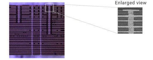
F-ALCS technology enables not only huge wiring capacity but also shortening of fabrication lead time.
03
IVH structure for over 500mm sized PCBs
By applying IVH technology for large size substrates (> 500 mm), the limitation of mounting of parts on the front and back sides and the limitation of wiring accommodation density by PTH vias are released.

 Application Fields & Structure
As a recent trend, demand for large-sized probe card PCBs with huge wiring capacity has grown as the wafer size gets larger and the simultaneous measurements DUT increase. We provide a variety of stub-less VIA structures and high speed transmission technology for the wafer testing of a state-of-the-art devices.
01
Technology Application
We provide optimized probe card PCB technology for the upgrading requirements, addressing the simultaneous measurements DUT increase and the fine pitch probing.
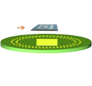
Image diagram
(Note) DUT: Device Under TEST
02
PCB Structures and their Strong Points
We propose a variety of PCB structures for upgrading specification requirements for probe cards.
The features for each PCB structure are shown below.
Strong points for each structure, in comparison with our products

03
Most Suitable Structure for Device Under Test
We propose optimized PCB structures for probe card requirements of semiconductor devices, addressing high speed operation, narrow pitch probing and simultaneous measurement DUT increase.
Suitable structures for each type of DUT

 Outline of PCB Specifications
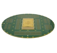
Organic PCB applications for probe card and its PCB specifications.
01
Organic Probe Card for Flash memory
| Layer Construction | 57 Layers (F-ALCS Technology) |
|---|---|
| PCB Size, Thickness | φ480mm, 6.2mm |
| # of Nets(Signal), R(Signal) | 20,700wires, R<2.0Ω |
02
Organic Probe Card for DRAM Memory
| Layer Construction | 74 Layers (F-ALCS Technology) |
|---|---|
| PCB Size, Thickness | φ520mm, 7.4mm |
| # of Nets(Signal) | 30,000wires(Signal) |
03
Organic Probe Card for Logic LSI
(Interposer Type, Multi Layer Organic PCB)
(Interposer Type, Multi Layer Organic PCB)
| Layer Construction | 42 Layers (7+28(F-ALCS)+7) |
|---|---|
| PCB Size, Thickness | 100×100mm, 2.7mm |
| # of Nets(Signal), R(Signal) | 500nets/DUT, 125µm,R<2.0Ω |
04
Organic Probe Card for Logic LSI
(Interposer Integrated Type)
(Interposer Integrated Type)
| Layer Construction | 76 Layers ((11-14-11)+40) |
|---|---|
| PCB Size, Thickness | φ280mm, 9.56mm |
| # of Nets, Pad Pitch | 750nets/DUT(Signal)、125µm |
 Related technology
Advanced Technologies
Back to top
Product
Back to top
Solution Services
Back to top
Technical Services
Back to top