APCS/SEMICON Japan 2022 Exhibition Guide
Thank you for visiting our booth. See you next year !
We will exhibit for the first time at the "Advanced Packaging and Chiplet Summit(APCS)" co-located with "SEMICON Japan 2022" at Tokyo Big Sight from the 14th to the 16th of December, 2022. This new summit will highlight leading-edge packaging technologies as they fuel semiconductor innovation.
Under the main theme of "The Future is Interconnected", we will showcase our advanced solutions applied to our PCBs for semiconductor equipment.
We hope to see you at our booth !
Exhibition Information
| Name of exhibition: |
Advanced Packaging and Chiplet Summit (APCS)
|
| Date: |
December 14 [Wed] - 16 [Fri], 2022 |
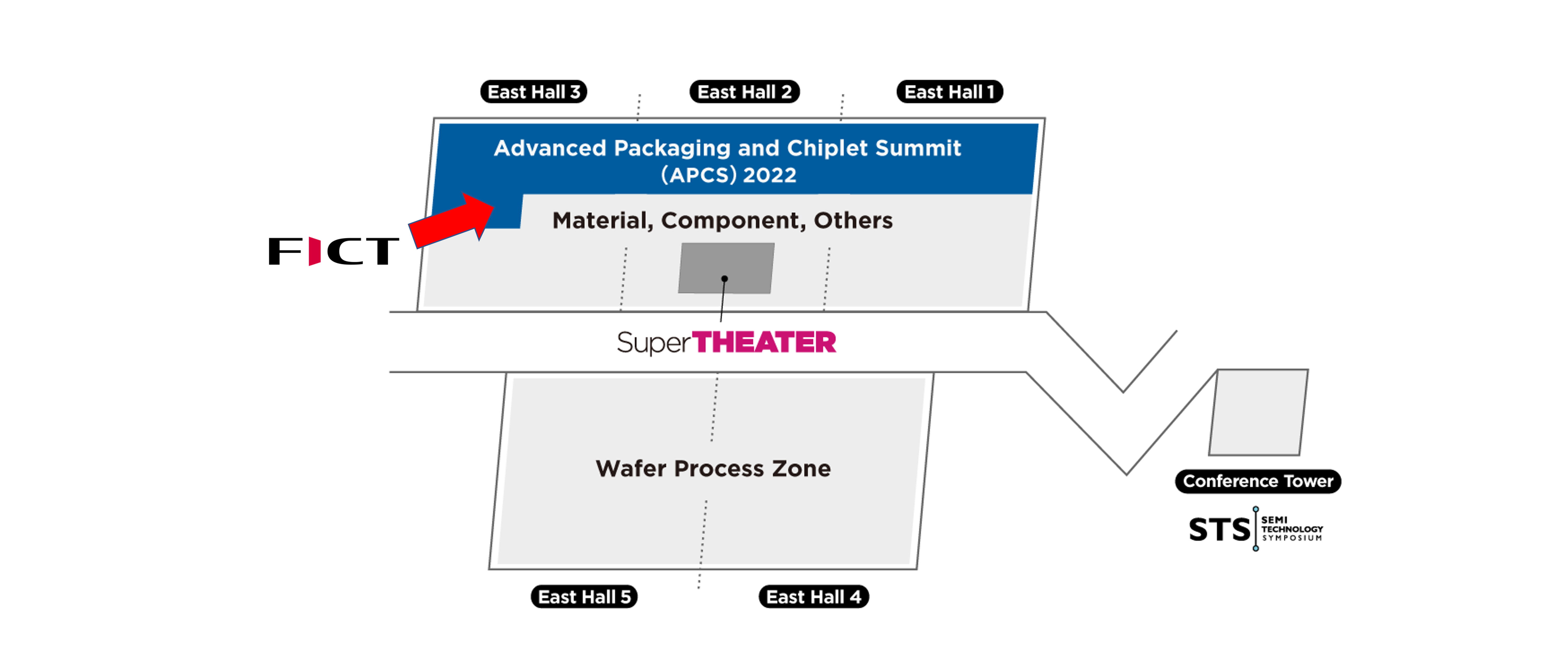
| Place: | Tokyo Big Sight East Hall 5 Address:3-10-1, Ariake, Koto-ku, Tokyo 135-0063 |
| Booth No.: | No.3845 |
| Registration: |
Online Registration is required to visit the exhibition. |
| Co-located Event |
Booth
Contents of the exhibition
Main theme: The Future is Interconnected
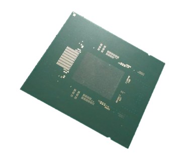
1.High end substrate package for Large FC-BGA PCB
We will exhibit a state-of-the-art large FC-BGA packaging substrate (□100mm) optimal for large Die and multi-chip packaging mounting.
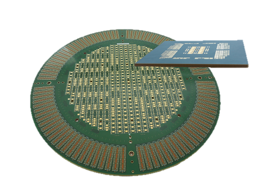
2. F-All Layer Z-Connection structure (F-ALCS)
We will exhibit our F-ALCS technology. With the use of a conductive paste for Any Layer IVH structure we can avoid the plating process and create 70+ layers PCBs by going though the laminating process just once.
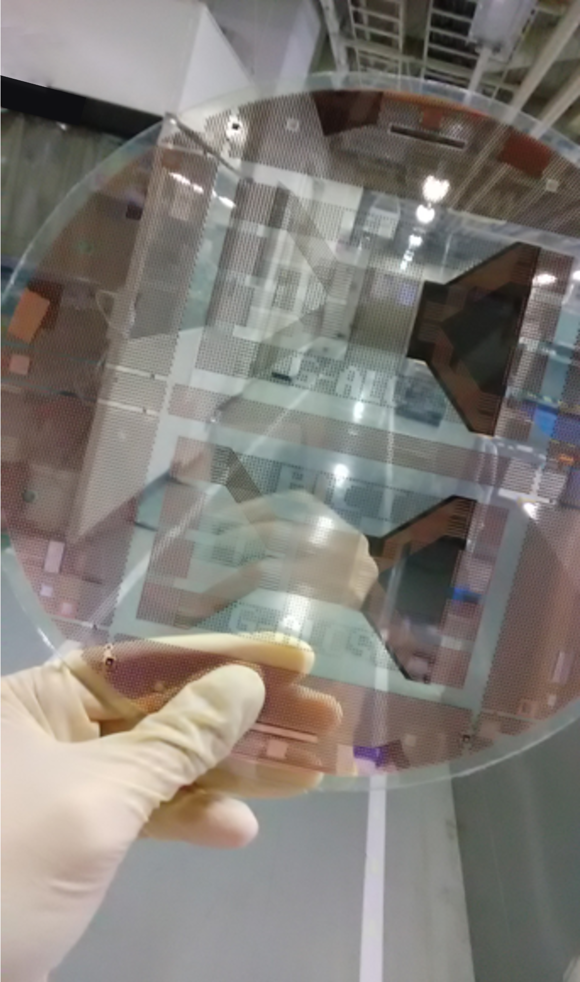
3.Glass All Layer Z-connection Structure (G-ALCS)
We will exhibit the Multilayer glass substrate prototype we created by bonding each glass PCBs with a resin and connecting all the layers with our F-ALCS technology.