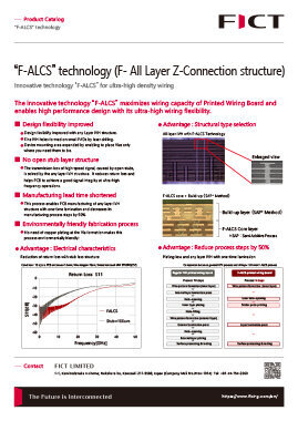


“F-ALCS” technology (F-All Layer Z-Connection structure)
The innovative technology "F-ALCS" maximizes wiring capacity of Printed Wiring Board and enables high performance design with its ultra-high wiring flexibility.
Download“G-ALCS” technology (Glass All Layer Z-Connection Structure)
New inorganic substrate : Multi glass core layers with conductive paste for customer’s specific needs for higher reliability.
DownloadGlass Core Package Substrate(New Concept)
Glass All Layer Z-Connection Structure (G-ALCS) Core with build-up layers for chiplet integration architecture.
Download

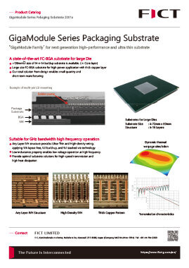
GigaModule Series
Packaging Substrate
A state-of-the-art large FC-BGA packaging substrate with >100 sq. mm size buildup is available for large Die and multi-chip packaging with small quantity and short-term manufacturing
DownloadTFC Embedded Substrate
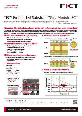
“GigaModule-EC”
GigaModule-EC, a best suitable packaging substrate with embedded thin film capacitor(TFC) for next high-performance & energy-saving semiconductor
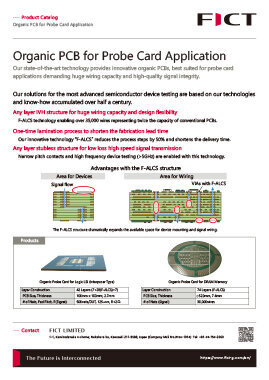
DownloadOrganic PCB for
Probe Card Application
Our state-of-the-art technology provides innovative organic PCBs, best suited for probe card applications demanding huge wiring capacity and high-quality signal integrity.
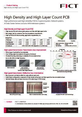
DownloadHigh Density and High Layer Count PCB
High-performance and High-reliability PCB for Supercomputers, Network systems, AI Data Center Servers and also Millimeterwave systems
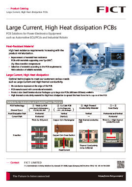
DownloadLarge Current,
High Heat dissipation PCBs
PCB Solutions for Power Electronics Equipment such as Automotive ECU/PCUs and Industrial Robots
Download

